Introduction
Electromagnetic Interference (EMI) is a disturbance in the electronic circuitry of a device that occurs when exposed to an electromagnetic (EM) field.
Integrating all these elements into a new system while ensuring compact form factor, heat dissipation, and reasonable assembly costs is challenging from a mechanical design perspective. There are also challenges related to EMI and EMC to consider when designing an HMI system. Finally, DFM/DFA are important aspects of HMI design as the system needs to be manufacturable at scale without overly complex assembly and costs. Here are some of the major HMI design challenges design teams need to overcome to create a scalable product.
Three of the most common EMI sources are radio frequency interference (RFI), electrostatic discharge (ESD), and power disturbances.
EMI typically refers to short-range interference that is caused by high frequency emissions within the device/system itself (Figure 1), while RFI refers to longer wavelength interference from external sources.
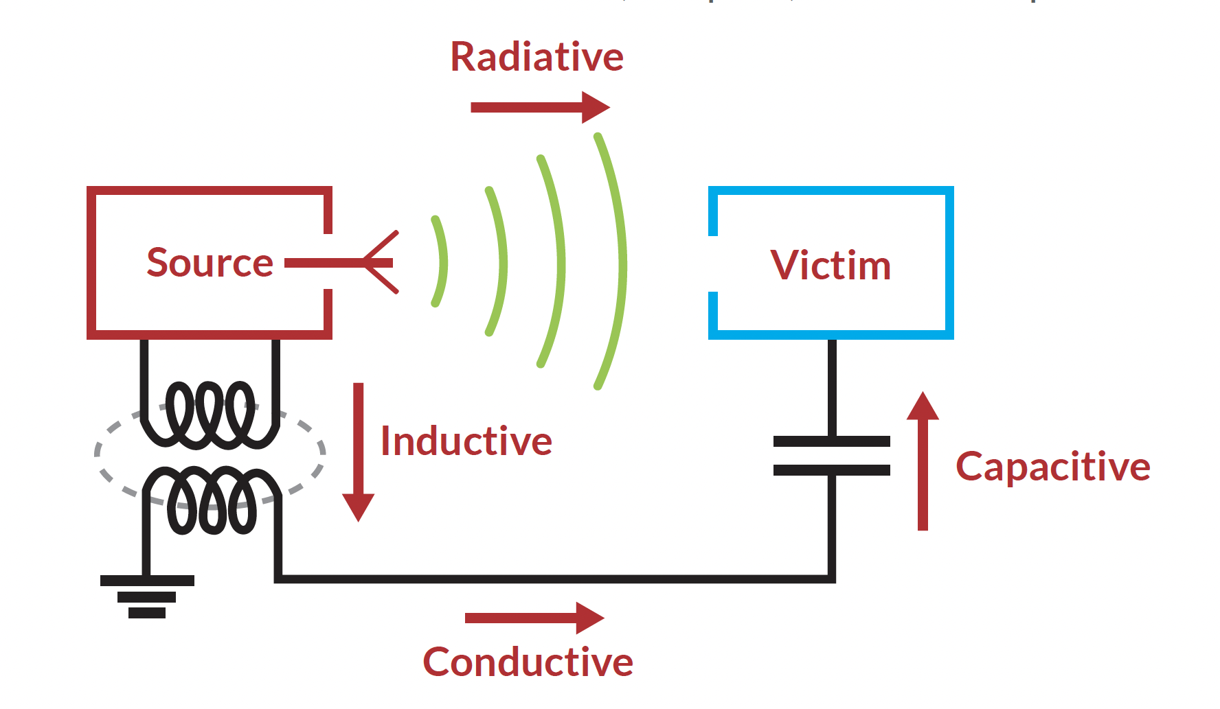
Figure 1. Electromagnetic Interference (EMI) can be radiated and/or conducted (image from Electrical 4U)
Because EMI can be damaging to product performance and safety, nearly all electronics sold in any market must pass some form of electromagnetic compatibility (EMC) standards.
A device’s conducted emissions must be within set limits for the proper functioning of another device or system. EMC testing limits are defined by various recognized standards bodies worldwide. These sets of standards include the International Electrical Commission (IEC), International Special Committee on Radio Interference/Comité International Spécial des Perturbations Radioélectriques (CISPR), and MIL-STDs (military standards)
Once a device proves through testing that it is within the limits, it is considered compliant with that particular set of standards. Which standards a device must meet depends on factors like where it will be sold and its intended market/application.
By following good EMI design and testing principles, such as correctly integrating various types of EMI shielding and using compliant components, designers can minimize EMI and pass compliance testing on the first try, which saves both time and money.
This post will outline some of the most reliable methods and solutions for doing so.
The Four Main Sources of Signal and Power Interference
When there is interference between electronic devices, signal and power line/wiring, and other electrical plant or process equipment, the unwanted noise can degrade critical measurement and control signals in the same system or even in nearby systems.
This is particularly risky in modern, dynamic industrial and factory environments with multiple systems of powerful equipment operating and communicating all at once.
Signal interference can be broken into four sources. Below, we outline each type and how it might be mitigated via design:
- Static Noise: When an electrical field distorts the signal
How to Mitigate: Continuous foil shields that will provide 100% shielding efficiency and aid in proper grounding techniques
- Magnetic Noise: Emanates from large AC motors, transformers, and knife switches and may set up current flows in opposition to the instrument
How to Mitigate: Twisted pair signal wiring.
- Common Mode Noise: Current flowing between different potential grounds located at various points within a system
How to Mitigate: A properly engineered/installed power and grounding system
- Crosstalk: The superimposing of the pulsed DC or standard AC signals between two or more nearby wires or cables
How to Mitigate: Individually shielded twisted pair cables
Which Industries are the Most Susceptible to EMI?
Every single application that involves electronics are at a risk of problematic EMI, but some markets are more susceptible than others due to the complexity and sensitivity of their devices. These include:
Measuring and Testing Methods for Tackling EMI in a Design
EMI testing is a valuable tool for designers to make sure a device or system is compatible with its electromagnetic environment.
If the right tests are chosen and correctly performed, testing will reveal the device/system’s real-world EMI potential. Good testing procedures will also allow designers to determine if a device will meet regulatory EMC standards.
There are two general types of EMI testing:
Pre-compliance Testing, which occurs during the design phase using a spectrum analyzer with near-field probes (Figure 3) to determine EMI levels. The boundary between near-field and far-field is usually within one wavelength.
Compliance Testing, in which an IEC-certified organization performs EMI emission compliance testing in an engineered environment, ensuring no incidental EMI from unrelated devices can enter.
Pre-compliance testing may reveal several types of EMI; designers can then use this information to employ the appropriate mitigation methods. These common types and methods for reducing them are as follows:
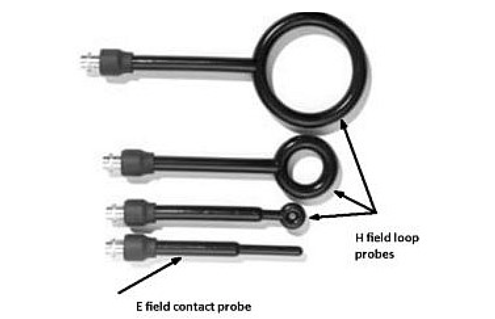
Figure 3. Near-field probes for a spectrum analyzer (Image from Test & Measurement Tips)
AC Field EMI: EMI caused by electrical AC fields can be reduced using adequate shielding of wire connections and cables. Twisted pair or coaxially-shielded cables can provide strong shielding.
Magnetically-Induced EMI: Conventional shielding is often enough to reduce magnetically-induced EMI. Another option is to put enough distance between the measurement circuit and known EMI sources which may be on the PC board or externally located.
EMI from Ground Loops: Poor grounding practices can result in currents that flow between different ground reference potentials in a measuring circuit, interfering with each other.
First, it’s important to note that ground wires from a sensor should not be shared with any other sensor or power load.
If this is not the issue, a grounded metallic shield for the instrumentation circuitry should help to suppress these ground loops.
Another possible solution is the use of twisted pair wiring. This works because each twist becomes a small loop antenna; the loop is reversed in the next twist, which cancels the interference from the first loop and so on.
Finally, it may also help for designers to place auxiliary power supplies close to the controller.
What Else Can be Done to Prevent EMI in Design?
Additional best practices to minimize EMI in the design of your device include:
- Shielding and other PC board methods can lower or eliminate offending EMI radiation to nearby electronics as well as to or from a circuit board.
- Make copper loop areas in PC board designs as minimal as possible; copper traces should avoid parallel runs.
- Avoid vias in differential copper traces.
- Remember: low inductance ground planes are important.
- Use guard and shunt traces for clock lines.
- Consider decoupling capacitors, especially with high frequency components.
A highly skilled Electronics Manufacturing Service (EMS) can help incorporate these best practices as well as provide additional solutions for OEMs.
PCI, for instance, has the expertise to help with antenna design, cellular technology for 5G, LTE, 2G, and 3G, Bluetooth, Wi-Fi, GNSS – GPS, GLONASS, Galileo, BeiDou, V2X, RF simulation, Vehicle communication for J1708, J1939 CAN, and multi-region regulatory compliance.
We follow the gold-standard guidelines of Design for Manufacturability and Assembly (DFMA) to minimize cost, ensure component availability, and expedites time-to-market.
Our Lean Six Sigma manufacturing expertise enables us to customize our manufacturing line to meet our partners’ requirements.
If needed, we provide our customers the flexibility needed to quickly scale production as needs arise. We provide our partners with high-quality products at lower manufacturing costs thanks to our shorter change-over time and leaner material control.
Contact PCI today to learn more about our capabilities.